Ignore Detection of Partial Discharge Failures NOW —
Pay Massive Amounts Later!
By Stephen Chaikin
High Voltage Isolation devices, such as optocouplers, can contain defects within their dielectric barrier yet still pass testing on traditional Hi-Pot/ATE test equipment. These devices can be returned from the field with dielectric breakdown at some future date, months or even years later, and become a fearful liability for a device manufacturer as well as for their customers. The consequences for businesses involved in Defense, Medical, Automotive, etc, can be disastrous.
In the automotive business we can all remember the PR nightmares that Toyota recently went through, with the series of recalls due to faulty parts and the following precipitous drop in sales.
With regard to the medical profession the repercussions resulting from the death of a person perceived by a failure in electronic instrumentation, are enormous. The damaging PR material propagated by the press, again resulting by a precipitous drop in sales, followed by expensive engineering testing to find the validity of the accusations are but a few that can take an enormous toll on the bottom line.
The problems are similar with NASA and the space shuttle except the scale is cosmic. Continual space shuttle problems, with the pull of public perception and on-going focus on cost savings, mixed with the backdrop of the perceived ineffectiveness of our administration can easily lead to the close down of the agency.
So what’s the problem? Theoretical dielectric strength values of insulating barrier materials would always apply if device manufacturers could produce consistently pure insulation barriers. Often, however, high voltage dielectrics contain defects like voids and inclusions of air or other impurities. These voids will have lower breakdown strength than the surrounding dielectric and will discharge, or arc (like a small capacitor) when their breakdown strength is reached. The discharge, however, is limited to the length of the void, and after discharging, will slowly recharge with the limited current available through the good dielectric. The void eventually recharges to the breakdown voltage and discharges again, as the process continues (like a relaxation oscillator) as long as the applied electric field remains high enough. These discharges are considered “partial” because they occur across the void in a limited portion of the length of the dielectric barrier. Partial discharges, which cannot be detected by leakage current measurements, can over time cause carbon tree paths in the insulation that eventually lead to complete insulation breakdown. The problem then, is to detect the presence of partial discharge during manufacturing test in order to prevent this phenomenon from degrading devices in the field.
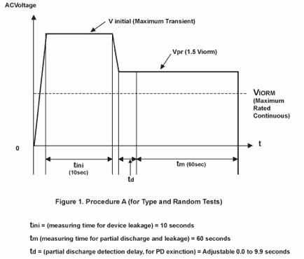
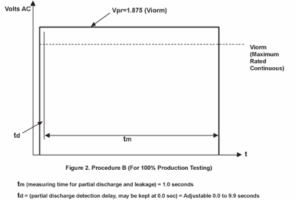
Partial Discharge measurement is used to evaluate the insulation integrity of an optocoupler. Partial discharge testing replaces the common dielectric withstand voltage test, because dielectric test voltages may pre-damage the insulation of an optocoupler. Partial discharge testing qualifies an optocoupler for operation at voltage levels that are below the inception level so that no harmful breakdown of the insulation occurs during its normal lifetime. The illustrations describe the partial discharge test for Type and Sampling (Procedure A) and for 100% production (Procedure B) testing in accordance with VDE 0884.
| Term | Definition |
|---|---|
| Vinitial | Maximum test voltage for the Partial discharge test. It is also the maximum transient over voltage occurring in a rated mains service class. At this initial voltage partial discharge (but no breakdown) may occur. Vinitial also equals Viotm (transient over voltage) |
| Vpr | Partial Discharge test voltage applied to an optocoupler and maintained for a specific time period, tst. During this time, Partial Discharge is measured at a specific time interval, tm. Vpr=1.5 X Viorm for procedure A and Vpr=1.875 X Viorm for Procedure B. |
| Viorm | Working voltage (maximum service insulation voltage); this is the maximum continuous permitted voltage that may be applied to an optocoupler. This value is specified by VDE to each insulator. |
| tm | Test time for Partial Discharge equal to 60 seconds for Procedure 1 and 1 second for procedure B. |
| tini | Time beginning at Vinitial test voltage, which equals 10 seconds. |
| td | Test voltage initialization time. |
| Pass/FailCriteria | No leakage failures and no optocoupler to have more than 5 pC Partial Discharge during Partial discharge test time, tm. |
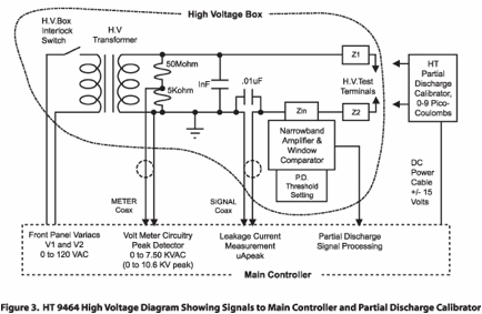
Figure 3 is an illustration of the High Voltage signal paths that are used by the HT 9464 Tester to obtain device leakage and partial discharge measurements. The primary of the H. V. transformer receives regulated constant voltage AC power from the settings of the front panel variacs V1 and V2 for a duration determined by front panel T1 and T2 test time settings. The secondary of the H. V. transformer applies the test voltage to the H. V. test terminal contacts in a handler. Not shown is the safety test site cover that is interlocked to the main controller to prevent operators from touching the contacts when high voltage is present. Notice that the H. V. path includes Z1 and Z2 in series with the contacts. Both of these consist of a 50Mohm resistor shunted by a 22pF capacitor. These limit the energy to the device contacts for the following reasons:
- Safety. The maximum 50/60 Hz AC current will be about 100uA. By comparison, perception of alternating current passing through the human body requires at least 0.5 mA.
- Less degradation to failed devices that may pass when retested at reduced voltage settings.
- Less high frequency radiation (that can disturb digital logic in both handler and tester) when shorted or arcing devices occur during testing.
Leakage Measurement. When a device is placed in the contacts the 50/60Hz current from the transformer high voltage secondary will pass through Z1, Z2 and Zin (less than one ohm) and through the SIGNAL coax to the leakage current measurement circuit in the Main Controller. The current will return in the coax shield to chassis ground and the H. V. secondary. The measured device peak current will be compared with the Leakage Threshold setting and the tester will produce a Fail Leakage if the measurement is excessive.
Partial Discharge Measurement. Because of the high frequency nature of partial discharges that may occur in the device under test, the associated current will take a different path than that of 50/60Hz leakage current. The 1 nanoFarad capacitor now becomes the low impedance high voltage source for partial discharge transient current that travels through the two 22pF shunt capacitors in Z1 and Z2 (and the device under test) to Zin (the first stage of the narrowband amplifier). Passing through Zin, transient current then goes directly through the 0.01 microfarad capacitor (bypassing the leakage measurement circuit) and returns to the bottom of the 1 nanoFarad capacitor. The narrowband amplifier will respond to the high frequency components that get amplified and sent to the comparator for amplitude discrimination. The comparator is referenced to a three digit partial discharge threshold setting that has been previously set with the Partial Discharge Calibrator (usually at 5 picocoulombs). If a partial discharge is detected by the comparator the red LED on the side of the H. V. Box will blink and the signal will be sent to the main controller for processing.
Setting the Partial Discharge Threshold requires the HT PDC700V Partial Discharge Calibrator that is capable of producing accurate 0 to 9 picocoulombs pulses that are used to set the three digit Partial Discharge Threshold adjustment. Normally the single digit thumb-switch on the calibrator is set to 5 picocoulombs. The calibrator spring contacts (pogo pins) are then placed against the handler contacts and the three digit partial discharge detection threshold setting on the side of the H. V. Box is increased until the red LED just stops blinking.
The Test Equipment required for Partial Discharge Testing is considerably different from the standard Automatic Test Equipment (ATE) utilized to test analog, digital and mixed signal circuits. The design must be able to generate high voltages (up to 10 kV peak) and detect leakage in the sub-mA range. Additionally for Partial Discharge measurement the equipment must have the ability to detect and measure minute charges at the picocoulomb level. For accurate and repeatable Partial Discharge measurements the equipment must be calibrated against a traceable standard. Additionally for use in production interfacing to a handler is mandatory. Last but not least the equipment needs to meet VDE and IEC standards.
HARRIS TUVEY (registered as HT, LLC) is a privately owned company that specializes in Semiconductor Equipment. The HT9460 and HT9464 product lines were previously owned by Hewlett Packard and were purchased by HARRIS TUVEY in 1998. HARRIS TUVEY is located near the heart of Silicon Valley. For further information:
| Website | www.ht-world.com |
| info@ht-world.com | |
| Phone | 650-207-6168 |
| Fax | 408-320-1110 |
With over 600 systems installed at major manufacturers of semiconductor devices, HARRIS TUVEY is the leading supplier of High Voltage and Partial Discharge Test Equipment.
Mr. Stephen Chaikin is Manager of Engineering for the High Voltage product line by HARRIS TUVEY.


